We harvest energy from
natural and artificial light
Dracula Technologies harvests ambient light to generate energy using specific, highly efficient organic materials that can capture both natural and artificial light. In low-light environments, our OPV devices have achieved high power conversion efficiencies.
This high performance is combined with long-term stability, even under accelerated aging conditions.
Thanks to their high performance even in low-light conditions, our OPV modules are ideally suited to indoor applications.
Benefits of Light Energy
Harvesting VS Batteries?

Environmentally friendly
- Light energy harvesting allows to reduce carbon emissions and environmental impact.
- Less recycling waste.
- No rare earths or heavy metals used.

Regulatory compliance
- By 2027, regulations will make the use of non-rechargeable batteries more restrictive (Directive 2013/56/EU of the European Parliament). As a sustainable solution, light energy harvesting complies with these regulations.

Lower TCO for B2B IoT use cases
- Elimination of multiple battery replacement costs.
- Optimizing return on investment (ROI) by reducing the costs associated with manual replacement.

Safe
- Ensures uninterrupted power for consistent operation.
- Free from chemical leakage or explosion risks found in batteries.
- Safe for all environments, zero hazardous emissions.
LAYER® is an organic photovoltaic module
What is it?
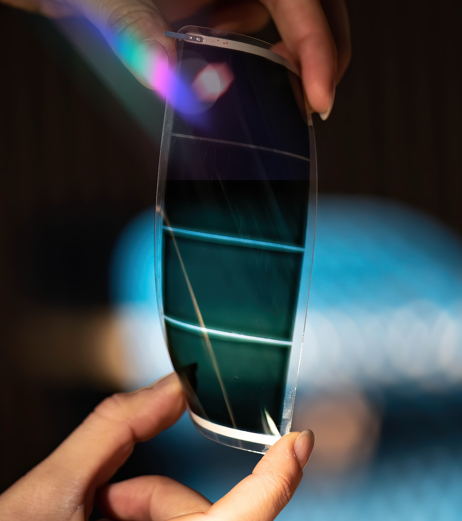
An indoor organic photovoltaic module is a device that converts energy from ambient light using an organic active layer composed mainly of carbon (C) and hydrogen (H). The adjective “organic” refers to this hydrocarbon composition.
The active layer absorbs light photons, generating electron-hole pairs. These pairs are then separated by an internal electric field, producing an electric current. The other layers of the organic module, such as the interfacial layers or electrodes, are designed to facilitate the extraction and collection of the charges created in the active layer.
These organic modules are part of the third generation of photovoltaic technologies, representing a significant advancement in the field of renewable energies. They offer potential advantages in terms of flexibility, low production cost and diverse applications compared with more traditional photovoltaic technologies.
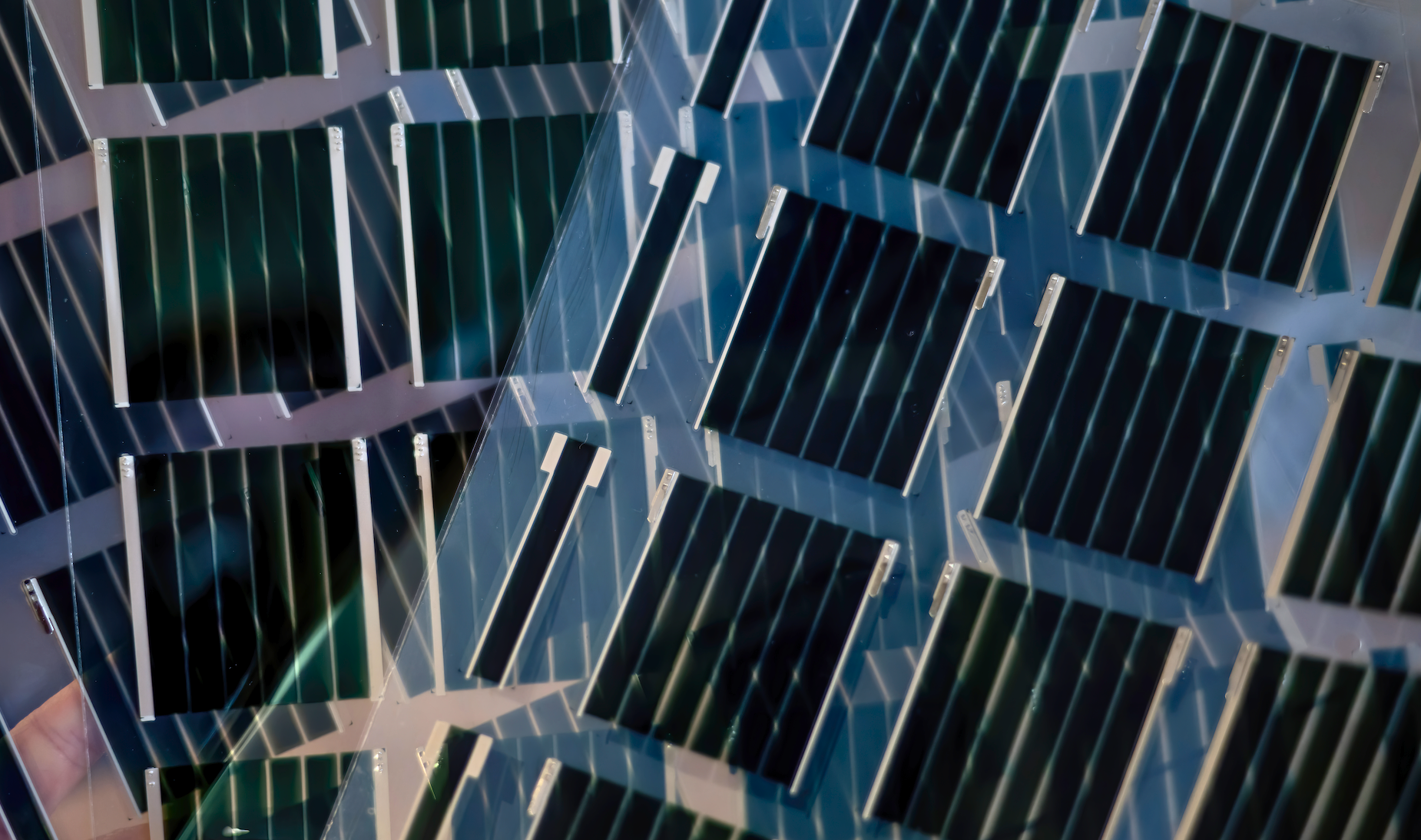
Product by Dracula Technologies
LAYER®
A BHJ* Cell Architecture
*Bulk Heterojunction
At Dracula Technologies, we offer an optimized device structure with exceptional performance. LAYER® is designed without a silver layer classically used in existing OPVs, which improves the absorption of light in the active layer, thereby optimizing the overall performance of the device.
Usually, an interfacial layer called Hole Transporting Layer (HTL) facilitates the extraction of holes from the active layer by the top electrode. In our configuration, the top electrode is specifically designed to ensure both extraction and collection of electrical charges.
Our technology uses the concept of Bulk Heterojunction (BHJ) where the active layer is comprised of a blend of electron-donating material and electron-withdrawing material in inverted device structure, widely used in organic photovoltaics (OPV).
This name derives from the need to use distinct materials to create electrical charges and facilitate their movement. This involves mixing an N-type polymer (donor) with a p-type organic material (acceptor), leading to the creation of a heterogeneous mixture. When these materials are combined, numerous junctions form between the acceptor and the donor in the active layer blend.
These multi-junctions, visible in the diagram, play an essential role in the conversion of light into electricity.
How do organic photovoltaic cells work?
The function of organic photovoltaics is similar to polycrystalline and monocrystalline silicon solar cells. They generate electricity thanks to the photovoltaic effect. It means they directly convert photons into electricity at the atomic level.
The process of photo-generation and charge transport to the external circuit inside a polymer-based photo-active layer can be divided into 5 stages.
Light absorption
Absorption of light in the active layer. The active layer contains two materials: A donor and an acceptor. Dracula Technologies uses only organic materials.
Exciton creation
Conversion of light into charge within the active layer: absorbed photons create coulombically bound electron–hole pairs known as excitons that require an additional driving force to separate into free charges.
Exciton diffusion
The excitons are not locally defined; they can diffuse along a polymer chain or between adjacent polymer chains. The diffusion length characterizes the distance an exciton can travel before recombination takes place. These excitons must dissociate prior to any recombination in the BHJ.
Charge separation
After the exciton arrives at the interface, charge separation takes place at the donor/acceptor interface. Separated charge carriers leave the interface, then by moving along a set of acceptor and donor sites arrive at the electrodes. The nano morphology of the active layer blend is of utmost importance for the efficiency of the charge separation.
Charge transport and collection
Finally, the separated charges must cross the photoactive layer/interfacial layers/electrode interfaces to reach the external circuit. The interfacial layers facilitate transport, but charge collection is ensured by the electrodes which generally have high conductivity.
Why is OPV one of the most suitable
technologies for indoor IoT applications?
No rare earths or heavy materials that are harmful to the environment: Organic photovoltaic modules (OPV) are safer for indoor environments where proximity to users is frequent.
LAYER® stands as the most environmentally friendly OPV solution, boasting the lowest Life Cycle Assessment (LCA) among all other OPVs.
OPV modules have a significant advantage in indoor applications because of the specific optical characteristics associated with this environment.
Most light sources used for indoor lighting are fluorescent lamps and white light-emitting diode (LED) lamps. These light sources emit light in wavelength ranges from 350 nm to 750 nm: in the UV-vis spectral range (visible spectrum of light). OPV modules are distinguished by their ability to absorb visible light efficiently: over 90% of organic molecules have an absorption capacity limited to the visible spectrum.
OPV module have a good spectral response in the visible region and are therefore the most suitable candidates for indoor applications. Outdoors, where the entire light spectrum is present (visible and non-visible radiation: UV and infrared), OPVs become less effective due to their limited absorption.
OPV efficiently generates energy from surrounding light sources.
The LAYER® technology produces energy even in low-light conditions, starting from 50 lux.
It is compatible with different indoor lighting sources due to the optimal absorption in the visible range of its organic materials.
Organic photovoltaic cells are lightweight and extremely thin (1000 times thinner compared to silicon solar cells).
This results in considerable savings on materials, making the devices more attractive from a cost perspective.
The high flexibility of the OPV devices make them easy to integrate into a variety of products, especially for applications requiring curved or flexible surfaces.
OPV panels offer great design flexibility.
LAYER® has a free-form capability, which means that thanks to our inkjet printing technology, we can create modules of any desired shape.
Thanks to inkjet printing technology, it is possible to increase the number of strips to adjust the voltage and current of the OPVs to the customer’s specific needs.
Our organic materials are very stable in ambient air, allowing the modules to operate for many years without degradation of performance.
The adequate encapsulation of our LAYER® modules guarantees a lifespan exceeding 10 years under indoor environment.
OPV modules are distinguished by their low production cost, making them extremely attractive for a diverse range of uses.
They are manufactured at low pressure and ambient temperature, resulting in a significant reduction in manufacturing costs.
For LAYER®, we use Inkjet Printing
What is it?
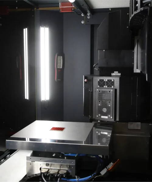
Drop-on-Demand (DoD) Inkjet Printing is a deposition technique that uses print heads equipped with nozzles (small orifices a few micrometers in diameter) to eject ink droplets in a meticulous manner, enabling the creation of precise patterns.
By incorporating piezoelectric materials into the printheads, mechanical deformations are induced by the application of an electrical voltage, causing the ink droplets to be ejected.
Accurate control of the shape and intensity of the applied voltage ensures consistent droplet ejection, guaranteeing precision and consistency in the printing process with each cycle.
At Dracula Technologies, we have developed our own specific formulations for each material, optimized to precisely match the characteristics of our printhead. The ink we use is based on carbon-based materials, making it environmentally friendly.
The 4-step
printing process
Ink preparation
The ink formulations for the different layers are prepared using green solvents. Specific additives are used to prepare stable ink and steady ink jetting allowing to obtain high quality films.
All formulations are proprietary to Dracula Technologies and do not use halogenated solvents.
Printing
The prepared ink formulations will subsequently be printed using industrial inkjet printers in ambient air without the need of controlled atmosphere to create the desired pattern.
A heat treatment is carried out leading to the formation of thin films. A stack of four layers is printed to finalize the OPV device.
Encapsulation
One of the most effective steps that can be taken to increase the lifetime of OPVs is their encapsulation, which protects them from atmospheric degradation (water and oxygen).
Efficient encapsulation is essential for long-term device performance.
LAYER® modules are encapsulated between two barrier films using a sheet-to-sheet process to guarantee a lifespan of 10 years.
Characterization
Once the OPV devices are encapsulated, they are ready for characterization. Measurements of the electrical current versus voltage (I-V) curves of a OPV cell or module provide a wealth of information.
For this, Dracula Technologies has set up indoor simulators to measure the electrical performance of LAYER® cells and modules under different indoor lighting conditions.
What are the advantages of Inkjet Printing?
A digital technique
Inkjet printing technology can be used to create organic photovoltaic (OPV) modules in custom shapes, tailored to specific customer requirements.
Indeed, this digital technology makes it possible to transform images into a functional layer to build an OPV module by converting the images into pixels and filling these pixels with droplets of ink.
Very easy to install
The inkjet printing process is simple to implement, allowing quick and efficient changeover from one image to another without the need for major equipment modifications.
The equipment itself remains unchanged (only images and materials can be modified depending on the product specifications), reducing the complexity of the manufacturing process.
Efficient material utilization
We print our modules using the so-called “sheet-to-sheet” inkjet printing process.
This approach requires reduced quantities of ink and represents an economical option in terms of material usage.
Unlike other competing technologies such as the roll-to-roll process, which requires printing large areas of material, the inkjet process works selectively using only what is strictly necessary.
This allows for efficient use of our raw materials, with less than one gram of material used to produce one square centimeter.

A technology secured by
a strong scientific background
With over 10 years of experience, Dracula Technologies
is the sole global player using inkjet printing for OPV technology.
is the sole global player using inkjet printing for OPV technology.
- 8 patents families
- 8 PhD
- 78 Scientific publications
- Login
- Sign Up
body::-webkit-scrollbar {
width: 7px;
}
body::-webkit-scrollbar-track {
border-radius: 10px;
background: #f0f0f0;
}
body::-webkit-scrollbar-thumb {
border-radius: 50px;
background: #dfdbdb
}


