A short overview of the third-generation solar cells: concept, materials, and performance.

Sadok Ben Dkhil
Most solar cells present on the market are based on silicon wafers, they are called first-generation technology. Second-generation cells are thin-film technologies that are often commercially available, such as copper indium gallium selenide (CIGS), cadmium telluride (CdTe), gallium arsenide (GaAs), and amorphous silicon (a-Si: H). Currently, inorganics like crystalline silicon, polycrystalline silicon (poly-Si), cadmium telluride, and copper indium germanium selenide with power conversion efficiency (PCE) of 15–20% are dominant in solar energy production.
Third-generation cells are less commercially advanced ‘emerging’ technologies. This includes organic photovoltaics (OPVs), copper zinc tin sulfide (CZTS), perovskite solar cells, dye-sensitized solar cells (DSSCs), and quantum dot solar cells.
During the past five years, organic and perovskite solar cells have reached points in their technological evolutions where large-scale deployment is possible, and this is the reason why I decided to focus on these two technologies which constitute two emerging technologies with more promising potential.
In a general photovoltaic device, the conversion starts with light-induced charge generation, followed by transport of the generated charges and collection of the charges by the electrodes. In this context organic and perovskite solar cells differ in the mechanism of charge generation due to the significantly different nature of the active layer materials (the layer that will absorb light and convert it into electricity), namely organic semiconductors and hybrid organic-inorganic perovskite. I will summarize the main operation principles of organic and perovskite solar cells, the materials, and discuss the advantages as well as the limitations of each technology.
It is however important to mention that both organic and perovskite solar cells, have the advantage to be processed by a great versatility of methodologies, including solution or vacuum processing techniques. Besides, both types of devices are built-in similar architectures and there is a growing trend for material from organic solar cells to be used in perovskite solar cells.
1. Organic solar cells
The first solar cell family that will be discussed is organic solar cells. These solar cells have photoactive layers comprising in general a semiconducting polymer and a fullerene derivative (or NFA for non-fullerene acceptor derivative) and have been the subject of several scientific publications. This family contains bulk heterojunctions (BHJs). “ A heterojunction is an interface between two different semiconducting materials”.
!! The current improvement from ≈2.5% in 2013 to 18 % in 2020 in organic solar cell performance is primarily credited to these novel non-fullerene acceptors (NFA).
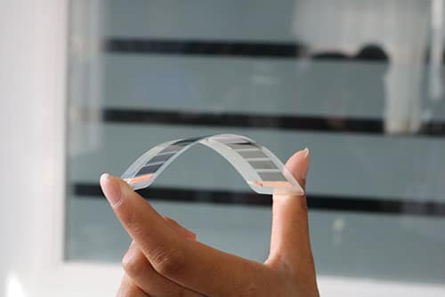
The organic photovoltaic devices hold some significant advantages over inorganic devices, including low cost of materials, lightweight, strong, and tunable absorption characteristics, flexibility, and the potential to be fabricated using roll-to-roll or sheet to sheet printing techniques. Unfortunately, some organic materials suffer from stability issues arising from photochemical degradation. Organic solar cells can be made transparent or different colors, but this will lower the overall efficiency.
The ability to make them flexible has some advantages in several markets but it means they are more susceptible to moisture and oxygen ingress that can cause degradation than if they had been laminated to glass.
What is an organic solar cell structure ?

Figure 1 : Schematic diagram of typical BHJ-OSC (Regular OSC, inverted OSC and tandem OSC)
Often an organic solar cell is built on a transparent conductive oxide (TCO) electrode material like indium tin oxide (ITO) substrate. In literature, commonly three types of organic solar cells can be found, and schematic representation is shown in the figure. In the so-called “Regular” or “standard” BHJ configuration, ITO is coated with a thin layer of hole transporting layer (HTL); on top of this HTL, a blend of donor and acceptor is coated, and then a thin electron transporting layer (ETL) and a low work-function metal cathode are usually vapor-deposited.
In the so-called “inverted” configuration due to the inverted polarity of charge collection, ITO is coated with a thin layer ETL, before a blend of donor/acceptor. A thin layer of HTL and high work-function metal anode are deposited on top of the BHJ blend.
Nevertheless, both of the abovementioned single-junction configurations can only achieve an efficiency maximum of ≈ 14–16% in the most favorable case due to either the lack of a broad absorption range of the donor/acceptor blend or limited charge carrier mobility, which require a thin (80–120 nm) blend for efficient charge collection. To avoid these limitations, two or more sub-cells with complementary and/or congruent photo absorption profiles are linked by a thin interconnecting layer (ICL) to construct a tandem configuration.
How do oganic solar cells work ?

Figure 2 : Simplified working principle of an organic solar cell
The process of photo-generation and charge transport to the external circuit within a polymer-based photoactive layer consisting of a donor and acceptor is well known in literature and can be separated into five steps (see figure 2). The first step is light absorption and photogeneration of an exciton (An exciton is an electrostatically bound electron-hole pair) within the active layer (donor and acceptor phases). It is important to note that exciton in conjugated polymers is not locally defined; they can diffuse along a polymer chain or between adjacent polymer chains.
The diffusion length characterizes the distance an exciton can travel before recombination takes place. These excitons must dissociate prior to any recombination in the BHJ. Since charge separation takes place at the donor/acceptor interface, the internal structure on the nanoscale of the active layer film is of utmost importance for the efficiency of the charge separation. If this nanomorphology of the active layer is not yet optimized, only a fraction of the excitons is able to find the donor/acceptor heterojunction interface at which exciton dissociation can take place which will limit the performance of the cell.
Once the exciton has dissociated the free electron and hole migrate to the cathode and anode, respectively. The migration may occur due to the driving force from the gradient in the chemical potentials of the electrons and holes at the donor-acceptor junction. Furthermore, charge concentration gradients can produce diffusion currents. Electron- and hole-blocking layers are often included in BHJ solar cells to direct the charge migration to the desired electrodes in order to decrease recombination. The photo-generated holes and electrons within BHJ photoactive layers migrate through interconnected donor and acceptor phases, respectively. In order to reach the respective electrode holes and electrons must avoid coming into contact at an interface and undergoing recombination.
Finally, the separated charges must cross the photoactive layer/electrode interfaces to reach the external circuit.
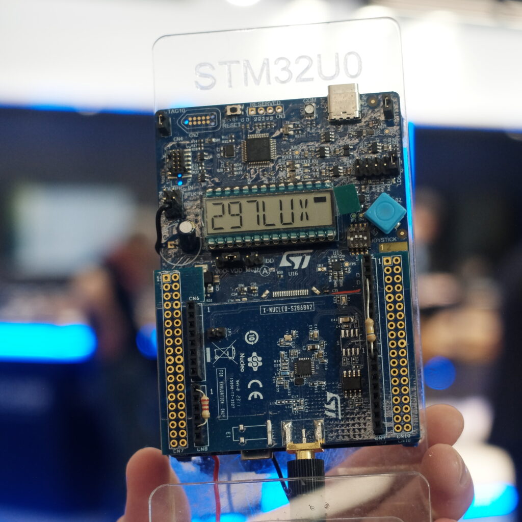
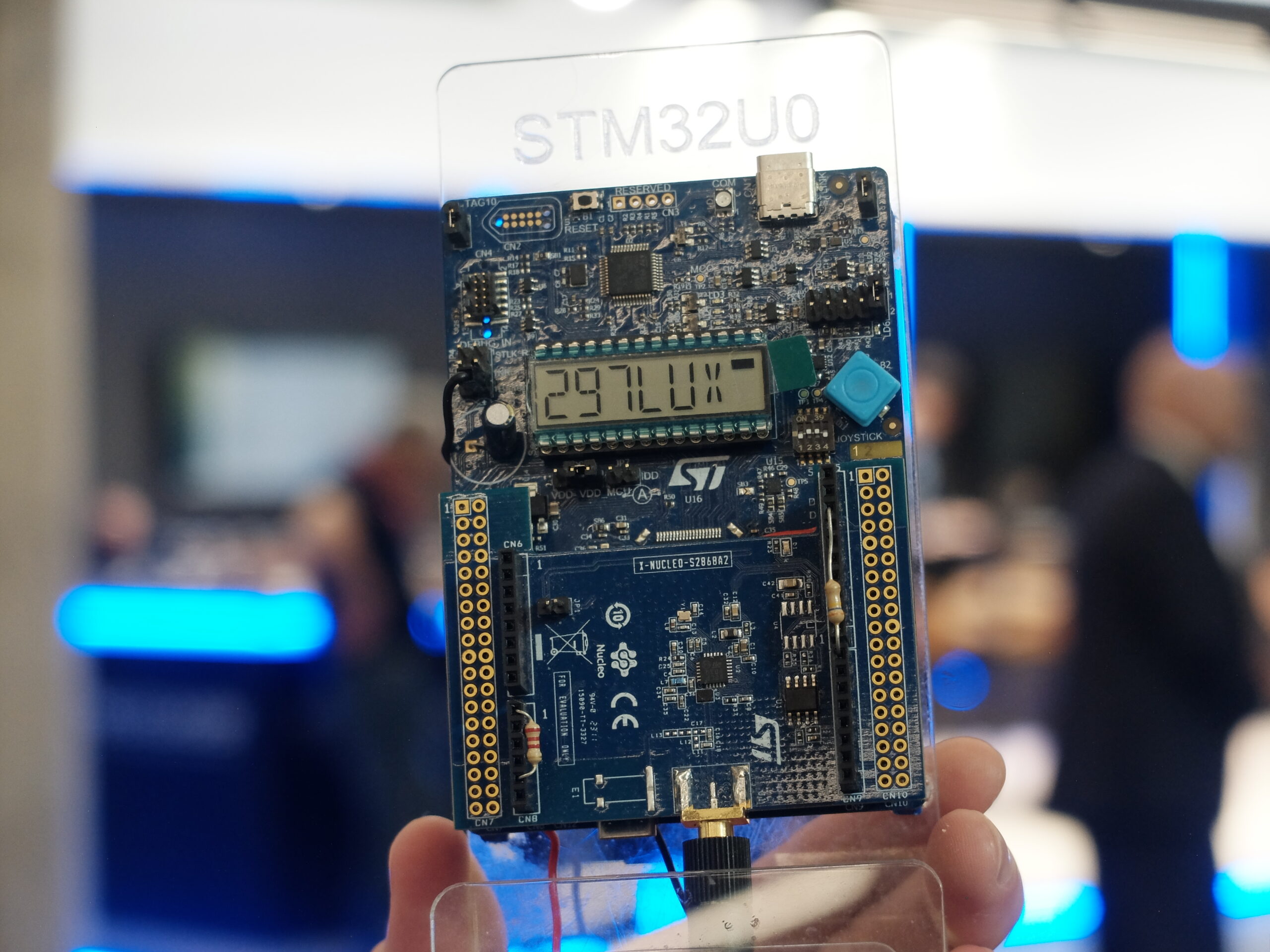
Organic photovoltaic technology is unlikely to challenge silicon’s dominance for large-scale electricity generation but offers promise in applications where lower cost, flexibility, weight, low energy requirement, durability, and low light conditions can be traded-off against efficiency. For example, the light-absorbing layer of organic solar cells provides flexibility so the cells can be tuned and optimized for different light spectra. This new approach to powering indoor applications could provide the Internet of Things with an inexpensive source of renewable energy, potentially replacing batteries. This particular role of organic cells for indoor applications will be discussed more in detail in the next newsletter.
2. Perovskite solar cells
Perovskite solar cells are new 3rd-generation solar cells that appear to have a very good chance of contributing to large scale solar energy production based on their high PCE and compatibility with scalable processes and are therefore included in this newsletter. Perovskite solar cells warrant discussion because never before in the history of solar cell research has such rapid progress in increasing the PCE been witnessed as that which has occurred for these solar cells.
Organic-inorganic lead halide perovskite is regarded as one of the ideal materials for photovoltaics ( At present there are different perovskite-type compounds which are not all very efficient), which demonstrated a certified power conversion efficiency (PCE) of 25.2% in 2019 surpassing the PCEs of the well-known high-efficiency thin-film solar cells based on copper-indium-gallium-arsenide or cadmium iodide (CdTe).
At present, the most challenging issue in perovskite solar cells is the long-term stability, which must be cleared up before putting it into practical applications. As we know that the stability of perovskite solar cells upon the severe environment, e.g., thermal treatment, light illumination, humidity, etc., appears to be the bottleneck that impedes their further commercialized. Among them, the humidity is demonstrated to be one of the possible causes of the degradation of perovskites. The commercialization of perovskite solar cells requires extensive research and development of new perovskite materials that are not only very effective in photoelectric conversion but also non-toxic and stable. Thus, in the next few years, more efforts are required for the development of inorganic lead-free perovskite solar cells.
What is a perovskite solar cell structure ?

Figure 3 : Four device configurations of PSCs: planar and mesoscopic structures.
A perovskite solar cell is a multi-layered device composed of a transparent conducting oxide (TCO) as a front electrode (in general based on FTO for Fluorine Tin Oxide) a light-absorbing perovskite layer, sandwiched between the N-type electron transport layer (ETL) and the P-type hole transport layer (HTL), and a metal back electrode. As shown in this figure, the perovskite solar cells can be fabricated in either a regular n–i–p or inverted p–i–n configuration and the former can be further divided into mesoporous and planar structures while the latter is usually planar. The selection of ETL and HTL is based on the workability of the energy-band alignment of the structure and the processing solvents.
How do Perovskite solar cells work ?
Contrary to that observed for organic solar cells, the absorption of photons in perovskite materials within perovskite solar cells does not lead to the formation of a large lifetime exciton. Numerous studies reported a small exciton binding energy for perovskite absorber in the range of a few milli-electronvolts, which indicates that practically the photon absorption leads to free carrier generation, unlike organic solar cells. This non-excitonic nature of the charge generation is crucial for the development of high-performance devices. The efficient generation of free electrons and holes in one step is one of the main advantages of perovskite solar cells since in excitonic solar cells significant losses in energy occur through exciton migration and exciton dissociation as explained in the operating mode of organic solar cells.
In perovskite solar cells charge separation can occur either by injection of photo-generated electrons into ETL or injection of holes in HTL. Furthermore, free electrons created near the perovskite/HTL interface have to diffuse through the entire width of the absorber layer before being extracted at the ETL/perovskite interface, with increased chances of recombination. Similar considerations apply to the holes near the ETL/perovskite interface.
To gain market share from crystal silicon solar cells, alternative technologies have to provide a desirable combination of high efficiency, low manufacturing costs, and excellent stability. Recent research suggests that perovskite solar cells have the potential to meet some of these conditions (particularly high efficiency and low manufacturing costs) and then become competitive in the marketplace. For that, an intensive research effort must be carried out in order to improve the stability of these new materials and avoid toxic derivatives.
Some example of companies working in the OPV and Perovskite devices manufacturing
So far, there are a few companies focusing on the development of perovskite solar panel: Microquanta Semiconductor, Solar-Tectic, Oxford Photovoltaics, Saule Technologies, and GreatCell Solar previously known as Dyesol.
The most key market participants involved in the manufacture of organic photovoltaic include Heliatek, InfinityPV ARMOR, Epishine, Sundew, and Dracula Technologies.